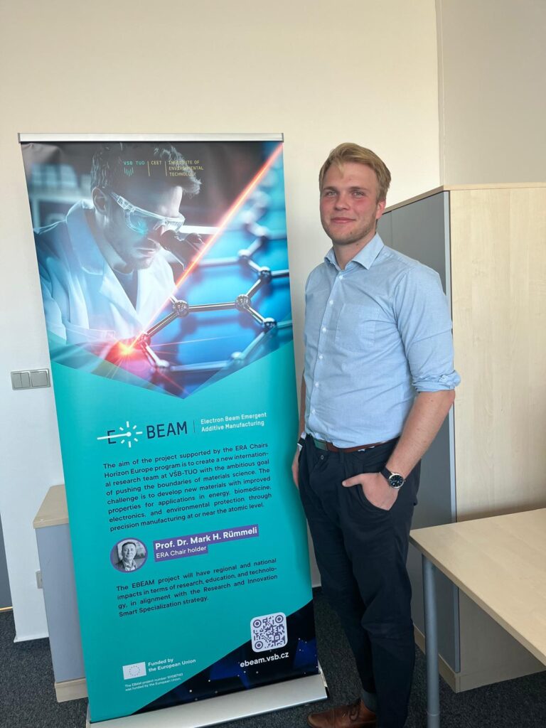
Ondřej Sakreida, a first-year PhD student at the Faculty of Materials and Technology at VŠB-TUO, joined the EBEAM team in October 2024. Despite needing to balance his research for the project with his studies, he was pleased to accept the offer to collaborate with ERA Chair project holder Marek Rümmeli. In this interview, Ondřej shares his expectations and tasks within the project.

What led you to a career in science?
I got into research and development while attending the secondary school in Opava which has quite strong ties to the industry. I was intrigued by research and discovering new things already there. I went on to study Nanotechnology at the Faculty of Materials and Technology at VŠB-Technical University of Ostrava, completing both my Bachelor’s and Master’s degrees there. In my Bachelor’s thesis, done in collaboration with the company TEVA, I focused on the development of pharmaceuticals. My Master’s thesis, done with French colleagues, aimed at developing a new material: copper modified with graphene for the aerospace industry. That was my first real encounter with the Nobel-prize-winning material, graphene. Now, I’m continuing my studies in a doctoral programme at the same faculty.
How did you start collaborating with Professor Marek Rümmeli on his EBEAM project?
The open position was recommended to me by the Director of the Centre for Nanotechnology, Gražyna Simha Martynková. Later on, Professor Rümmeli and I met, and he offered me the position.
What attracted you to this opportunity?
The technology at the heart of the EBEAM project could, in my view, fundamentally change the society. As a nanotechnologist, I’ve seen a lot of methods for controlled material and nanomaterial preparation, so I know it’s a complex process, and many methods turn out to be unsustainable, energy-intensive, and create numerous by-products. In contrast, methods like EBEAM allow us to use electron beams for highly precise preparation with extreme accuracy. This is an unprecedented technology that could open up a wide range of applications in energy, electronics, the semiconductor industry, and beyond.
So, the biggest appeal for you was the chance to work on something completely new?
That’s incredibly attractive to me as a young researcher. I believe there’s a real chance we could make a breakthrough in a specific field or in preparation methods. At the same time, I’m thrilled to work in an international team under the guidance of a world-renowned researcher. It’s almost unbelievable how much I’ve learned just in the first few weeks of this collaboration. Another big advantage is the opportunity to work with state-of-the-art microscopes, which we’ll even have the chance to modify ourselves. That’s a unique opportunity you don’t get everywhere. All this is very appealing.
What is your role in the project?
My task is to develop technologies and focus on the development of materials that can be used in them. Initially, we will likely focus on graphene and doped graphene production, as it is a highly sought-after material with unique properties for many applications.
Have you worked on anything similar, or is this entirely new for you? What expertise did you need to demonstrate?
I’d say I’ve done similar work, but not within one project. I used an electron microscope extensively for analyses in Teva while still in secondary school, as well as for analysing various materials during my university studies. I also worked on graphene production via chemical vapour deposition. These competencies likely played a role in my acceptance into the project.

